
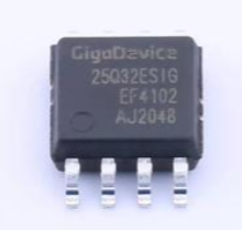
GD25Q32E
- Product brand :
- GD;Category:

- Manufactory model :
- GD25Q32E
- Packaging specifications:
- SOP-8 / USON-8 / WSON-8 / TFBGA-24
- Data Manual :
-
GD25Q32E Click to download
- Packaging method :
- Tape & Reel (TR) / Tray / Tube (Tape & Reel for standard orders)
- Product Consulting :
- Online message QQ:
Product Description
DS-00437-GD25Q32E-Rev1.5 Functional Description
GD25Q32E is a 32Mbit (4MB) SPI NOR Flash serial memory chip launched by GigaDevice. It supports Standard/Dual/Quad SPI interface with a maximum clock frequency of 133MHz, featuring XiP (Execute-in-Place), 100,000 program/erase cycles, 20-year data retention, software/hardware write protection, OTP security area and other functions. It is suitable for embedded systems, IoT devices, MCU firmware storage, industrial control and other scenarios, and is available in SOP8, USON8 and other packages.DS-00437-GD25Q32E-Rev1.5 is the Rev 1.5 datasheet for GigaDevice GD25Q32E, a 32 Mbit SPI NOR Flash memory.
1. Basic Storage Specifications
Capacity: 32 Mbit (4 MByte)
Organization:
Uniform 4 KB sectors
Uniform 32 KB / 64 KB blocks
256 bytes per page (page programming unit)
2. Interface & Speed
Interface: Supports Standard SPI / Dual SPI / Quad SPI
Standard: SCLK, CS#, SI, SO, WP#, HOLD#
Dual/Quad: IO0~IO3 multiplexed as bidirectional data lines
Max clock frequency: 133 MHz
Bandwidth:
Dual I/O: 266 Mbps
Quad I/O: 532 Mbps
Supports XiP (Execute-in-Place): high-speed continuous read, suitable for direct code execution from Flash by MCUs
3. Operating Performance (Typical)
Page programming: 0.5 ms
Sector erase (4 KB): 45 ms
Block erase (32/64 KB): 0.15 / 0.25 s
Chip erase: 12 s
Endurance: ≥ 100,000 program/erase cycles
Data retention: 20 years (typical)
4. Power & Power Consumption
Supply voltage: Single 2.7V ~ 3.6V
Standby current: 12 μA
Deep Power-Down current: 1 μA
5. Security & Protection
Software/hardware write protection:
Block protection range configured via status register bits BP0~BP4
Hardware lock of protection bits via WP# pin
Supports top/bottom block protection
Unique ID: 128-bit unique chip ID
Security registers: 3×1024-byte OTP security area (lockable)
SFDP register: compliant with standard parameter table
6. Control Functions
Write Enable / Write Disable (WREN/WRDI)
Read Status Register / Write Status Register (RDSR/WRSR)
Erase / Program Suspend and Resume
HOLD# pause: suspends communication without deselecting the device
Software reset
7. Package & Temperature
Packages: SOP8, USON8, WSON8, TFBGA24, etc.
Temperature range:
Industrial: -40℃ ~ +85℃
Extended temperature: -40℃ ~ +105℃ / 125℃
8. Typical Applications
Embedded firmware, BIOS/UEFI, configuration data storage
IoT devices, MCUs, set-top boxes, gateways, industrial control, consumer electronics
Non-volatile code/data storage requiring high speed, low power consumption, and small package
Product Details
TAG:
Similar products
Prev: AN206 Instructions for Scatter Loading in Keil MDK5 for GD32MCU_Rev1.1
Next: DS-00484-GD25Q64E-Rev1.6